- 您现在的位置:买卖IC网 > Sheet目录307 > ADP3419JRM-REEL (ON Semiconductor)IC MOSFET DVR DUAL BOOTST 10MSOP
�� �
�
�ADP3419�
�to� the� MOSFET� data� sheets,� Q� HSGATE� =� 18.6� nC� and�
�Q� LSGATE� =� 68� nC.� Given� that� f� MAX� is� 300� kHz,� P� MAX� would�
�be� about� 130� mW.�
�Part� of� this� power� consumption� generates� heat� inside� the�
�ADP3419.� The� temperature� rise� of� the� ADP3419� against� its�
�environment� is� estimated� as:�
�The� total� MOSFET� drive� power� dissipates� in� the� output�
�resistance� of� ADP3419� and� in� the� MOSFET� gate� resistance�
�as� well.� η� represents� the� ratio� of� power� dissipation� inside� the�
�ADP3419� over� the� total� MOSFET� gate� driving� power.� For�
�normal� applications,� a� rough� estimation� for� η� is� 0.7.� A� more�
�accurate� estimation� can� be� calculated� using:�
�D� T� [� q� JA�
�P� MAX�
�h�
�(eq.� 4)�
�where� θ� JA� is� ADP3419’s� thermal� resistance� from� junction�
�to� air,� given� in� the� absolute� maximum� ratings� as� 220� °� C/W�
�for� a� 4� ?� layer� board.�
�h� [�
�Q� HSGATE�
�Q� HSGATE� )� Q� LSGATE�
�0.5� R1�
�R1� )� R� HSGATE� )� R�
�)�
�0.5� R2�
�R2� )� R� HSGATE�
�)�
�Q� LSGATE�
�Q� HSGATE� )� Q� LSGATE�
�0.5� R3�
�R3� )� R� LSGATE�
�)�
�0.5� R4�
�R4� )� R� LSGATE�
�(eq.� 5)�
�where:�
�R1� and� R2� are� the� output� resistances� of� the� high-side� driver:�
�R1� =� 1.7� (DRVH� ?� BST),� R2� =� 0.8� (DRVH� ?� SW).�
�R3� and� R4� are� the� output� resistances� of� the� low-side� driver:�
�R3� =� 1.7� (DRVL� ?� VCC),� R4� =� 0.8� (DRVL� ?� GND).�
�R� is� the� external� resistor� between� the� BST� pin� and� the� BST�
�capacitor.�
�R� HSGATE� and� R� LSGATE� are� gate� resistances� of� high-side� and�
�low-side� MOSFETs,� respectively.�
�Assuming� that� R� =� 0� and� that� R� HSGATE� =� R� LSGATE� =� 0.5,�
�Equation� 5� gives� a� value� of� η� =� 0.71.� Based� on� Equation� 4,�
�the� estimated� temperature� rise� in� this� example� is� about� 22� °� C.�
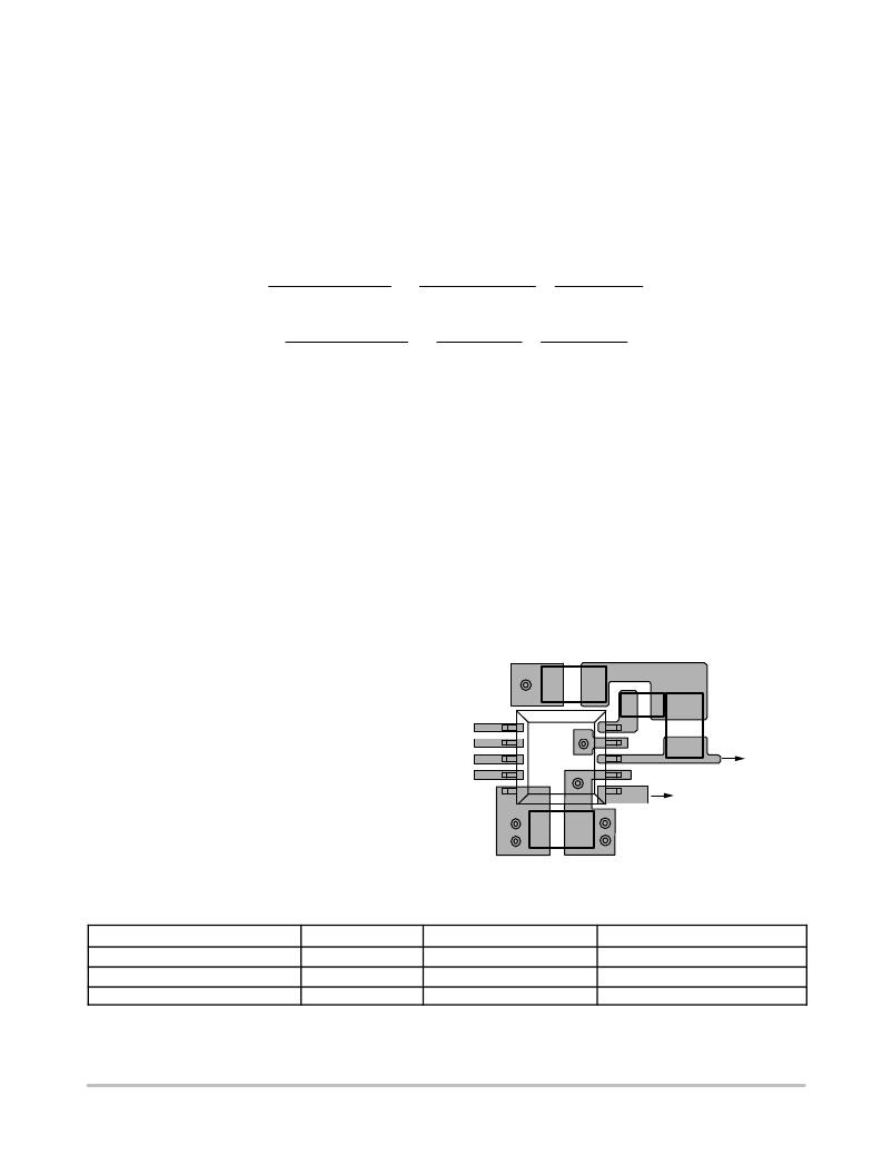
�PC� Board� Layout� Considerations�
�Use� the� following� general� guidelines� when� designing�
�printed� circuit� boards.� Figure� 17� gives� an� example� of� the�
�typical� land� patterns� based� on� the� guidelines� given� here.�
�?� The� VCC� bypass� capacitor� should� be� located� as� close� as�
�possible� to� the� VCC� and� GND� pins.� Place� the�
�ADP3419� and� bypass� capacitor� on� the� same� layer� of� the�
�?� It� is� best� to� have� the� low-side� MOSFET� gate� close� to�
�the� DRVL� pin;� otherwise,� use� a� short� and� very� thick�
�PCB� trace� between� the� DRVL� pin� and� the� low-side�
�MOSFET� gate.�
�?� Fast� switching� of� the� high-side� MOSFET� can� reduce�
�switching� loss.� However,� EMI� problems� can� arise� due�
�to� the� severe� ringing� of� the� switch� node� voltage.�
�Depending� on� the� character� of� the� low-side� MOSFET,� a�
�very� fast� turn-on� of� the� high-side� MOSFET� may� falsely�
�turn� on� the� low-side� MOSFET� through� the� dv/dt�
�coupling� of� its� Miller� capacitance.� Therefore,� when� fast�
�turn-on� of� the� high-side� MOSFET� is� not� required� by� the�
�application,� a� resistor� of� about� 1� W� to� 2� W� can� be� placed�
�between� the� BST� pin� and� the� BST� capacitor� to� limit� the�
�turn-on� speed� of� the� high-side� MOSFET.�
�D1�
�board,� so� that� the� PCB� trace� between� the� ADP3419�
�VCC� pin� and� the� MLC� capacitor� does� not� contain� any�
�R� BST�
�C� BST�
�via.� An� ideal� location� for� the� bypass� MLC� capacitor� is�
�near� Pin� 5� and� Pin� 6� of� the� ADP3419.�
�?� High� frequency� switching� noise� can� be� coupled� into� the�
�VCC� pin� of� the� ADP3419� via� the� BST� diode.�
�Therefore,� do� not� connect� the� anode� of� the� BST� diode�
�to� the� VCC� pin� with� a� short� trace.� Use� a� separate� via� or�
�trace� to� connect� the� anode� of� the� BST� diode� directly� to�
�the� VCC� 5.0� V� power� rail.�
�ORDERING� INFORMATION�
�TO� SWITCH�
�NODE�
�SHORT,� THICK� TRACE�
�TO� THE� GATES� OF�
�LOW-SIDE� MOSFETS�
�C� VCC�
�Figure� 17.� External� Component� Placement� Example�
�Device� Number�
�ADP3419JRM� ?� REEL�
�ADP3419JRMZ� ?� REEL�
�ADP34190091RMZR�
�Branding�
�P9A�
�P9B�
�P9B�
�Package� Type�
�10� ?� Lead� MSOP�
�10� ?� Lead� MSOP�
�10� ?� Lead� MSOP�
�Shipping� ?�
�3000� Tape� &� Reel�
�3000� Tape� &� Reel�
�3000� Tape� &� Reel�
�?For� information� on� tape� and� reel� specifications,� including� part� orientation� and� tape� sizes,� please� refer� to� our� Tape� and� Reel� Packaging�
�Specifications� Brochure,� BRD8011/D.�
�*The� “Z’’� suffix� indicates� Pb� ?� Free� part.�
�http://onsemi.com�
�9�
�发布紧急采购,3分钟左右您将得到回复。
相关PDF资料
ADP3611JRMZ-REEL
IC MOSFET DRIVER DUAL 10-MSOP
ADP5501ACPZ-RL
IC LED DRVR WHITE BCKLGT 24LFCSP
ADP8863ACPZ-R7
IC LED DRVR WHIT BCKLGT 20-WLCSP
ADUM1100UR
IC DIGITAL ISOL/COUPLER 8SOIC
ADUM1201CR
IC ISOLATOR DIGITAL DUAL 8SOIC
ADUM1210BRZ
IC ISOLATOR DIGITAL DUAL 8SOIC
ADUM1233BRWZ-RL
IC ISOLATR DGTL 2CH 0.1A 16-SOIC
ADUM1234BRWZ-RL
IC ISOLATR DGTL 2CH 0.1A 16-SOIC
相关代理商/技术参数
ADP3419JRMZ
制造商:Analog Device 功能描述: 制造商:Analog Devices 功能描述:MOSFET Driver, Dual, 10 Pin, Plastic, TSSOP
ADP3419JRMZ-REEL
功能描述:功率驱动器IC DUAL SYNCHRONOUS DRV RoHS:否 制造商:Micrel 产品:MOSFET Gate Drivers 类型:Low Cost High or Low Side MOSFET Driver 上升时间: 下降时间: 电源电压-最大:30 V 电源电压-最小:2.75 V 电源电流: 最大功率耗散: 最大工作温度:+ 85 C 安装风格:SMD/SMT 封装 / 箱体:SOIC-8 封装:Tube
ADP3419JRMZ-REEL1
制造商:AD 制造商全称:Analog Devices 功能描述:Dual Bootstrapped, High Voltage MOSFET Driver with Output Disable
ADP34200002RUR
制造商:Rochester Electronics LLC 功能描述:- Bulk
ADP3421
制造商:AD 制造商全称:Analog Devices 功能描述:Geyserville-Enabled DC-DC Converter Controller for Mobile CPUs
ADP3421JRU
制造商:AD 制造商全称:Analog Devices 功能描述:Geyserville-Enabled DC-DC Converter Controller for Mobile CPUs
ADP3421JRU-REEL
制造商:Rochester Electronics LLC 功能描述: 制造商:Analog Devices 功能描述:
ADP3421JRU-REEL7
制造商:ON Semiconductor 功能描述: